
The surface micromachining technology makes thin micromechanical devices on the surface of a silicon wafer. Large numbers of devices can be inexpensively made, and this technology integrates well with electronics. On the surface of a silicon wafer, thin layers of structural and sacrificial material are deposited and patterned. At the end of the processing the sacrificial material is removed, and completely assembled micro mechanical devices remain.
References are given as (p xxx) which refer to page xxx in the book "Micromechanics and MEMS"
This technique was first demonstrated in 1967 by H C Nathanson, W E
Newell, R A Wickstrom, and J R Davis using gold with a sacrificial photoresist
layer (p 21). In 1983 R T Howe and R S Muller demonstrated this technique
using polysilicon with a sacrificial silicon dioxide (p 505). Below
is a picture from Howe and Muller's original article (p 506)
At the Transducers '87 Conference two groups presented the
use of surface micromachining techniques to make micromechanical devices,
see M Mehregany, K Gabriel, and W Trimmer (p 509) and L Fan, Y Tai, and
R Muller (p514). A typical process sequence is shown below (p 515).

First a sacrificial silicon dioxide is deposited on the wafer and patterned,
then a structural layer of polysilicon is deposited and patterned.
This polysilicon layer will become structural elements such as gears.
Other layers are then deposited and patterned making the rest of the structure.
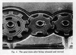
Etching in buffered hydrofluoric acid, HF, removes the sacrificial layers
leaving the gears shown below (p 511).
Surface Micromachining is being used in commercial products such as accelerometers to trigger air bags in automobiles.